![[Drool picture of ASM-1 frontplates]](asmdream.gif)
Originally Gene produced and sold the PCB. As of October 2002 he passed this work over to Laurie Biddulph <elby_designs@ozemail.com.au> who's site you find at http://www.elby-designs.com/. Be sure to visit Laurie's site NOW! Laurie has great ambitions on taking up the ASM-1 flag and raising it further, and what I see looks promising.
The PCBs is done in a real PCB shop and has a high quality and I strongly recommend them. To get PCBs please contact this fellow. Below follows information from Gene regarding the PCB.
Please note that I, Magnus, in no way is affiliated with the PCB selling. I provide information about this only as a friendly gesture to Gene, Laurie and those interested in attaining a PCB from him. My recommendation to get the PCB is as a fellow DIY person. I don't have any PCBs to sell, I only got what I needed for my own personal DIY usage.
What you get is a circuit board, plus documentation with a parts list, circuit description, and building hints.
The circuit board is professional quality - double-sided, soldermasked, silkscreened, and drilled with plated-through holes. No components are installed or provided. It is up to the builder to provide all circuit components, power supply, enclosure, and front panel. All components should be fairly easy to purchase in local stores or via mail-order.
Enjoy!
Magnus
| Spec's | ||
|---|---|---|
| Circuit board dimensions | 11" by 4.9" | |
| Power requirements | -15 Volts, Ground and +15 Volts | |
| VCO | inputs | 6 frequency |
| 2 linear FM | ||
| 2 pulse width | ||
| 1 sync | ||
| outputs | 1 sawtooth | |
| 1 rectangular | ||
| VCF | inputs | 4 cutoff CV+ |
| 1 cutoff CV- | ||
| 4 signals in | ||
| 1 Q pot in | ||
| outputs | 1 lowpass | |
| 1 bandpass | ||
| 1 highpass | ||
| 1 notch | ||
| 1 Q pot out | ||
| VCA | inputs | 1 +signal in |
| 1 -signal in | ||
| 3 amplitude control CV | ||
| outputs | 1 output | |
| ADSR | inputs | 1 gate in |
| 6 pot connections | ||
| outputs | ADSR out | |
| LFO | inputs | 1 rate input |
| LFO | outputs | 1 triangle out |
| 1 square out | ||
| Noise Source | outputs | 1 White noise out |
| 1 Pink noise out | ||
| 1 Random voltage out | ||
| Glide buffer | inputs | 1 CV in |
| 1 glide pot in | ||
| outputs | 1 glide pot out | |
| 1 CV out | ||
NOTE: All IC's are standard DIP packages.
| Count | Component type |
|---|---|
| 5 | CA3140 |
| 4 | CA3080 |
| 19 | Dual op-amp, TL082, LM358, etc. |
| 2 | LM311 |
| 2 | CD4002 |
| 2 | CD4053 |
| 2 | 2N4856 N-channel JFET |
| 6 | 2N3904 NPN transistor |
| 2 | 2N3906 PNP transistor |
NOTE: All trimpots should be multi-turn (10, 20, 25, etc.). All trimpot locations on the circuit board are 3-hole inline pattern with 0.10" (100 mil) spacing between holes.
| Count | Trimpot type |
|---|---|
| 13 | 100 kohm trimpot |
| 2 | 10 kohm trimpot |
| 1 | 100 ohm trimpot |
| Count | Component type |
|---|---|
| 6 | 1N4148 Diodes or equivalent (1N914) |
| 4 | 22 ohm 1% 0.25 W metal film resistor |
| 6 | 220 ohm 1% 0.25 W metal film resistor |
| 1 | 390 ohm 1% 0.25 W metal film resistor |
| 2 | 470 ohm 1% 0.25 W metal film resistor |
| 2 | 680 ohm 1% 0.25 W metal film resistor |
| 10 | 1 kohm 1% 0.25 W metal film resistor |
| 2 | 1.5 kohm 1% 0.25 W metal film resistor |
| 3 | 2 kohm 1% 0.25 W metal film resistor |
| 1 | 2.2 kohm 1% 0.25 W metal film resistor |
| 2 | 3 kohm 1% 0.25 W metal film resistor |
| 2 | 3.3 kohm 1% 0.25 W metal film resistor |
| 8 | 10 kohm 1% 0.25 W metal film resistor |
| 4 | 15 kohm 1% 0.25 W metal film resistor |
| 2 | 18 kohm 1% 0.25 W metal film resistor |
| 3 | 20 kohm 1% 0.25 W metal film resistor |
| 1 | 27 kohm 1% 0.25 W metal film resistor |
| 1 | 33 kohm 1% 0.25 W metal film resistor |
| 5 | 47 kohm 1% 0.25 W metal film resistor |
| 2 | 56 kohm 1% 0.25 W metal film resistor |
| 51 | 100 kohm 1% 0.25 W metal film resistor |
| 1 | 150 kohm 1% 0.25 W metal film resistor |
| 2 | 200 kohm 1% 0.25 W metal film resistor |
| 1 | 270 kohm 1% 0.25 W metal film resistor |
| 1 | 330 kohm 1% 0.25 W metal film resistor |
| 2 | 390 kohm 1% 0.25 W metal film resistor |
| 8 | 560 kohm 1% 0.25 W metal film resistor |
| 7 | 1 Mohm 1% 0.25 W metal film resistor |
| 4 | 1.5 Mohm 1% 0.25 W metal film resistor |
| 2 | 2 Mohm 1% 0.25 W metal film resistor |
| 2 | 18 pF capacitor |
| 2 | 30 pF capacitor |
| 4 | 100 pF capacitor |
| 2 | 330 pF capacitor |
| 1 | 1 nF capacitor |
| 2 | 2.2 nF capacitor |
| 3 | 10 nF capacitor |
| 24 | 100 nF capacitor |
| 2 | 1 uF capacitor, unpolarized |
| 2 | 4.7 uF tantalum capacitor, 16V |
| 2 | 10 uF tantalum capacitor, 16V |
| 2 | 100 uF electrolytic capacitor, 16V |
| Count | Component type |
|---|---|
| 2 or 3 | 1 kohm or 2 kohm +3300ppm/C tempco resistors |
| 2 | MAT-02 matched NPN pair (or equalent) |
NOTE:
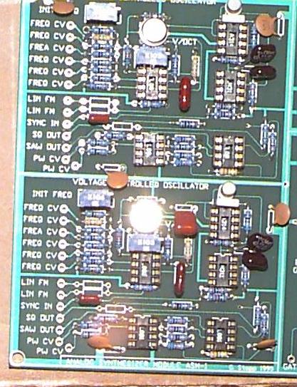
Overview Picture (Contributed by Roy Tate 2000-02-01, with a sligth editing touch by Magnus Danielson)
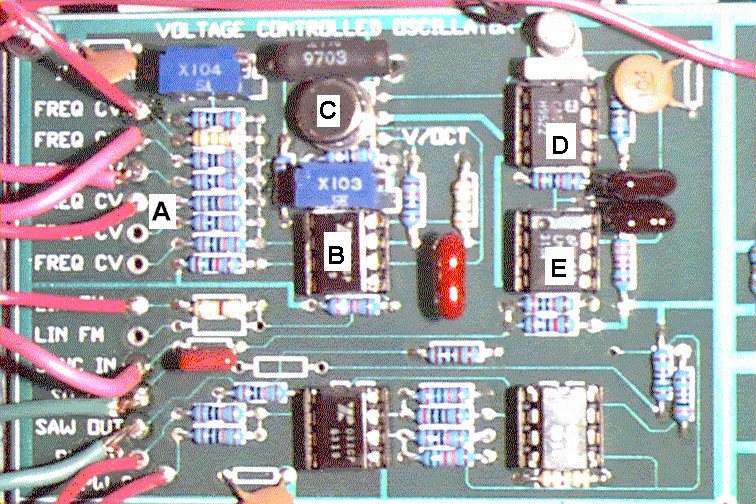
Closeup Picture (Contributed by Roy Tate 2000-02-01, with a sligth editing touch by Magnus Danielson)
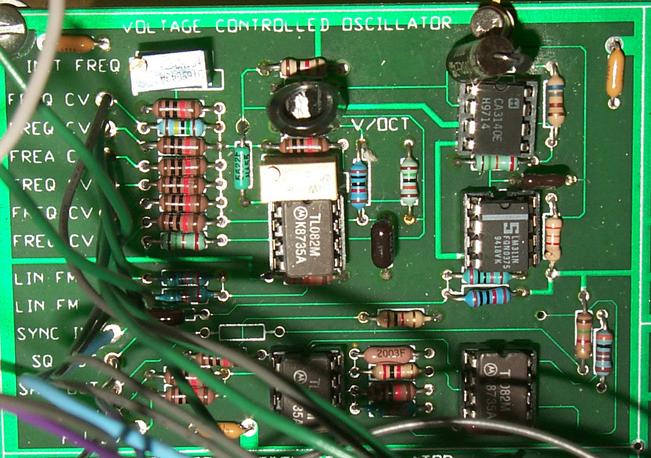
Closeup Picture (Contributed by Doug Ferrell 2000-02-02)
The VCO is an exponential sawtooth-based design substantially borrowed from Electronotes. It consists of a control voltage summing amplifier (U1A), driving an op-amp/NPN-pair exponantial current source (Q1, Q2 and U1B), which feeds a buffered-capacitor integrator (U3 and C3) with a FET discharge (Q3), controlled by a fast comparator (U4).
The control voltage amplifier is built around a virtual ground current summer based on the op-amp U1A, the resistor R8 and the pot P2. The scaling is set such that a sensitivity of 1 V/Oct is acheived when sent through a 100k Ohm resistor. The actual scale over the R13/R14 resistor divider needs to be slightly more than 1 V/Oct and due to divider chain imperfections the P2 is used to trim the actual gain of the summer. This is sensed as a scale trimming. The offset trimmer P1 is used to set the (externaly) unmodulated tone.
The oscillator core is really a current controlled oscillator with the MOSFET op-amp CA3140 (U3) and capacitor C2 acting as an integrator of the input current (pulled by Q2). The voltage of such an integrator can be described as
         Q
          C2     1    /
V    = - --- = - --  | I   dt
 out     C       C  /   in
          2       2
Since the input current does not change sign must the integrator be reset in order to restart the waveform, this is done by letting the comparator LM311 (U4) compare the output to the reference voltaged created out of the Vpp (15V) by the resistor divider of R19 and R20 thus giving the reference voltage of 5 V:
          R20             10k          10k       1       1
V    = --------- V   = --------- V   = --- V   = - V   = - 15 = 5 V
 ref   R19 + R20  PP   20k + 10k  PP   30k  PP   3  PP   3
When output of the CA3140 goes above Vref, the comparator LM311 will pull its output transistor collector (pin 7) to -15 V since its emitter (pin 1) is hooked to -15V. This will bias the JFET (Q3) into conducting range and reset the capacitor C2 through the Rds(ON) of the JFET. This exponential decay must be maintained for sufficently long in order to reach approximately 0V. The residue charge at the end of the reset period will create a part of a residue offset of the waveform. The time for the reset is set by the R18 and C3 and is set to one third of that of Rds(on) and C2.
Due to the lost integration time that occurs during the reset time will the reset time of approximate 1.5 us be compensated by a series resistor (R17) also known as a Franco compensation. This works by increasing the start level of the integration by Iin * R17 and thus compensates for the integration that should have happend during the time from when the JFET was enabled to when it was disabled. By dimensioning R17 to perfectly match the time of the lost time and tracking errors due to reset time integration blindness may be removed (well, reduced). This is also known as high frequency tracking error since it is only for highfrequency waveforms the fixed reset time becomes large part enough of the cycle. The fix will infact convert the time/frequency error into an waveform offset error.
t      = C2 * R17 = 2.2 nF * 680 Ohm = 1.496 us
 reset
The CCO will integrate from 0 V up to Vref and then reset. Given that the input current Iin is a DC current we can express this as
       1  /          1
V    = -- | I   dt = -- I   t
 ref   C2 /  in      C2  in  int
leading to
                1    1         1
t    = V    C2 --- = - V   C2 ---
 int    ref    I     3  PP    I
                in             in
giving the frequency
              3 * I
        1          in
f    = ---- = -------
 osc   t      V   * C2
        int    PP
which gives for Iref = 10 uA
        3 * 10 uA
f    = ----------- = 909.0909 Hz
 osc   15 * 2.2 nF
which is just above A5 at 880 Hz. The actual calculation of the nonmodulated frequency of the oscillator is
     3 * I          3 * V
          in             PP          3
f  = -------- = -------------- = --------
 0   V   * C2   R15 * V   * C2   R15 * C2
      PP               PP
The original value of R15 was 1.5M Ohm giving an Iref of 10 uA and a f0 of 909.09 Hz. This was later changed to a 150k Ohm resistor thus giving an Iref of 100 uA and a f0 of 9090.09 Hz. For a R15 of 1.5M Ohm would the A5 (880 Hz) be a suiteable reference tone to trim down to, for a R15 of 150k Hz would the C#9 (8869.844 Hz) be a suiteable tone to trim down to (see frequency trimming modification below).
The P1 trimmer has the problem that it is being scaled by P2 trimmer, so trimming P2 will affect the offset trim which makes the trimming procedure difficult. The P1 has infact a double duty to trim both the CV offset which is being sent into the summing amplifier when no other voltage is applied. It also has the duty to correct the frequency offset that comes from the reference current and the actual capacitor value. The reference current is formed by the voltage over the R15 resistor, which is 15V over 150k Ohm thus giving 100 uA of reference current. By inserting an extra trimpot of 10k Ohm in series with R15 one can pull down the unmodulated frequency (unmodulated means 0V input to the Q1 base, thus just mirroring over Iref to Q2). The new pot will allow for easy adjustment of the unmodulated frequency of the oscillator to hit a suitable note. By first adjust this unmodulated frequency can the scale (P2) and later the real note offset (P1) be adjusted with easier procedures and with better precission.
The five-volt unipolar sawtooth is inverted (U2B, R21 and R23) and level shifted (R22) to produce a ten-volt bipolar sawtooth for output. Another comparator (U5A) is used to produce a variable-width rectangular waveform from the sawtooth, with its own pulse width control voltage summing amplifier (U2A).
Regarding the components - take a look at the schematic for the VCO, starting at the upper left. This is the frequency control voltage input summing amplifier structure. The full frequency range of the VCO can be swept with a control voltage from -15 volts to +15 volts (higher voltages means higher frequencies) applied to any of the 100 kohm input resistors. The 100 kohm resistor to the Initial Frequency trimpot does not have to be precise. In fact you can leave off this resistor and the trimpot if you want to rely on the front panel controls for all VCO tuning. However I personally leave these trimpots in, first because they allow the front panel controls to be set to a comfortable range and matched between the VCOs, and second because they allow frequency control when bench testing the circuit board without a front panel attached at all. As for the remaining input resistors - you can see that they all have identical function, and you can put whatever you want here. I would recommend at least one high-value resistor (1 M, 1.5M, etc) for a Fine Tune front panel pot, plus one non-precision 100 kohm resistor for a Coarse Tune pot. For control from a keyboard or MIDI-CV converter, I would recommend matched precision 100 kohm resistors for at least those inputs. You can use non-precision 100 kohm resistors for CV inputs that need the full sweep range without any precision. You can use higher resistance for inputs with less sweep range.
Op-amp U1 can be a TL082, LM358, 1458 or whatever. It's not really critical.
The 15 kohm resistor at the (+) input of the CV summer is supposed to be equal to the parallel resistance of all resistors connected to the (-) input. You can get away with 10 kohm, 18 kohm, whatever, or just a wire (zero ohms). The resistor is just good op-amp practice.
The 100 kohms resistor/10 kohms trimpot combination is used to tweak the base of transistor Q1 to 18 mV change for 1 Volt change at the 100 kohms input. A tempco resistor can be used in the location shown, and you can mess around with the components values all you want as long as you keep the 18 mV/1 Volt ratio. See the notes elsewhere on tempcos.
The 150 kohms, 10 kohms, 390 kohms, 100 pF parts in the exponential converter should all be kept at these values. For Q1 and Q2 you can use 2N3904s. The closer matched they are, the better. The silkscreen on the PCB shows a MAT-02 from Analog Devices - this is the perfect part but is expensive. You can experiment with other NPN pairs at your own risk. The 560 kohm input resistors for linear FM can be made whatever value you want, with smaller resistance allowing for wider FM sweeps. 560 kohms is just copied from Electronotes.
The CA3140 cannot be substituted, nor can the LM311 (notice the weird pinouts on the LM311). Keep all values in this section the same as shown. The 20 k/10 k resistor divider at the (-) input of the LM311 is used to set the +5 Volt peak of the sawtooth waveform. You can mess with these using precision resistors to make for a precise five volts here, or use another 2-to-1 ratio divider if you don't have the rigth resisitors. Don't deviate too far from five volts here, as this will affect the VCO scale. The 2.2nF capacitor in the integrator should be a good cap - polystyrene, polycarbonate, etc., not too critical but just not some crappy ceramic piece of junk. The value can be messed with - a larger value will lower the overall frequency of the VCO, and a lesser value will increase the overall frequency range. Don't go overboard here, because the rest of the VCO is designed around this value.
The integrator discharge FET can be a 2N4856, 2N4391 or 2N4392. There may be more N-channel JFETs that work just as well, but these I have tried.
Op-amp U2 should be a TL082. If you use an LM358 here the sawtooth will get messed up starting around 12 KHz and just go downhill at higher frequencies, which will also mess up the subsequent PWM circuitry. Resistor values for the pulse width modulation control voltage summer at U2-A or the sawtooth level shifter at U2-B can be messed with, as long as you keep the ratios the same. Notice that the 560k to -15V is not the perfect value to center the 10V sawtooth exactly around ground - 620k may be better. You can always hand-pick a 560k and another resistor and make a little tee-pee thing in the mounting holes it you're really anal about the sawtooth symmetry about ground.
Op-amp U5 should be a TL082 for decent rectangular waveshapes. Notice that U5-B is a spare op-amp, and I tied it as a buffer to the raw sawtooth just so I didn't leav the spare pins floating. The 2k/2M resistors on the pulse comparator can be any values, as long as a fairly high ratio is maintained. The 2k/1.5k divider on the output does a 3-to-1 attenuation from the 30V output to a 10V output whilst maintaining a 1k output impedance.
The Sync input cap value probably isn't too critical, but I've only tried 100pF and that works fine.
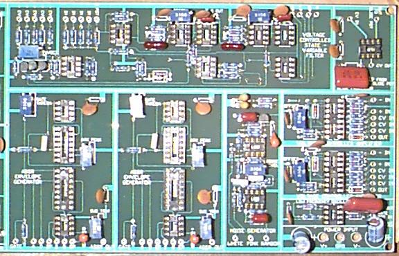
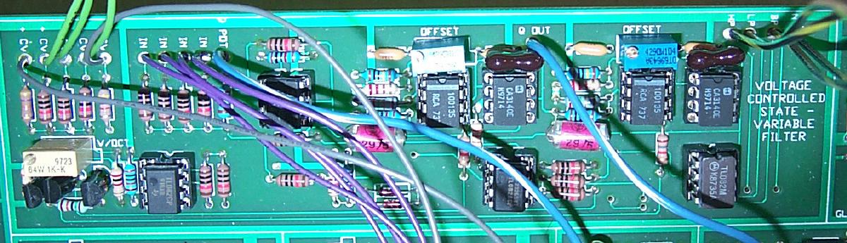
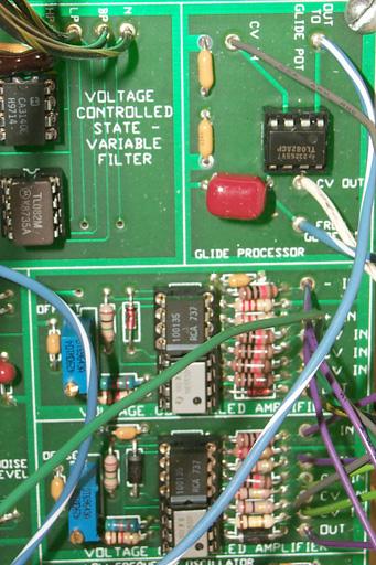
Overview Picture (Contributed by Roy Tate 2000-02-01)
Closeup Picture (Contributed by Doug Ferrell 2000-02-02)
The VCF is a State-Variable design, with exponential voltage-to-frequency response at 1 volt per octave (1V/oct). Lowpass, Bandpass, Highpass and Notch outputs are provided. Q is variable via panel control.
Regarding the components - take a look at the schematics for the VCF, starting at the upper left. This is the frequency control voltage input summing amplifier structure. The full frequency range of the VCF can be swept with a control voltage from -15V to +15V (higher voltage means higher frequencies) applied to any of the 100k input resistors. As you can see, they all have the identical function, and you can put whatever value you want here. I would recommend one non-precision 100k resistor for a Coarse Tune pot. For control from a keyboard or MIDI-CV converter, I would recommend matched precision 100k resistors for at least those inputs. You can use non-precision 100k resistors for CV inputs that need the full sweep range without any precision. You can use higher resistances for inputs with less sweep range. An inverting amplifier is provided to allow positive modulation voltages to drop the VCF frequency, and because I had an extra op-amp. A 47k resistor is shown on the input to this inverter, which means that this input will have twice the "normal" sensitivity, or 0.5 volts per octave. You can put the traditional 100k value here, or a higher value. My intention here is to use a panel pot as attenuator for modulation depth control, both on the inverting modulation input as well as on one of the positive inputs with a 47k resistor as well. Notice that since the envelopes from the ADST envelope generators are 15V amplitude, at full strength into a 47k input (either positive or negative) you will get just over 30 octaves of sweep! This is a bit much so attenuation is essential for cutoff modulation by envelopes.
The 2k feedback resistor can be a normal metal film type for non-critical work. On a VCF it matters a lot less than in a VCO. The 1.8k resistor at the (+) input of the summing amp is just good op-amp practice, and can be wired (zero ohms) without much effect. The 100 Ohm trimpot should be 10- or 20-turn for the best tweakability.
The signal input resistor can be 100k for unity gain of the VCF. However, if you run the VCO inputs straight in, the filter will distort a little, sounding like an MS-20 with the VCO's at full volume. I'd recommend putting input level controls on all four inputs - you'll be glad you did. The trimpots and 1M resistors at the (+) inputs of the 3080s are there to trim the DC offset. They may not be needed what with modern 3080 quality but I left them in. If you are thinking about leaving them out, try it first. If the VCF has too much DC offset on its outputs, put them in.
The divider/diode thing around the Q pot is a feedback limiter, duplicated from the schematic for the Oberheim SEM. It keeps the Q oscillation from clipping. You can experiment here, but it works as drawn. The Q pot is just a divider so it can be anything from 5k to 1M. The 100k resistor around the Notch output summing amp can be any value between say 10k and 1M, just keep them all the same, and match them with a DVM if possible for the best notch.
All other components should be kept the same. There is some leeway on the 330pF caps in the 3140 integrators - you can use sligthly smaller or larger ones, just make sure they're identical. Use good caps here (not ceramic).
The output buffers are required since the 3140 is a little wimpy driving into the negative region. I would add 1k output resistors (at the panel jacks would be okay) to keep all output impedances in the system at the same 1k value. I just forgot to add them on the circuit board.
I have long had a hidden page on the ASM 1 VCO, with lots of pictures from a tripp I did with an oscilloscope. You will find it here.
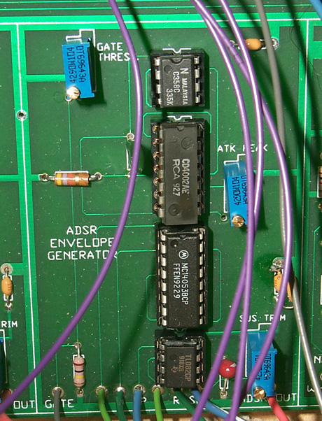
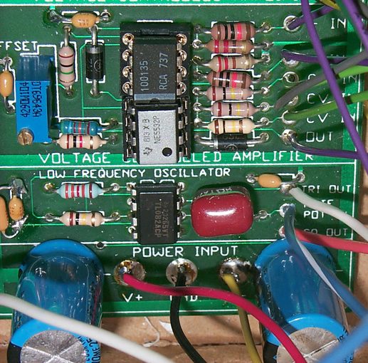
Closeup Picture (Contributed by Doug Ferrell 2000-02-02)
USe all values as drawn. Notice that the ADSR output is also lacking the 1k output resistor - this can be added at the panel jack.
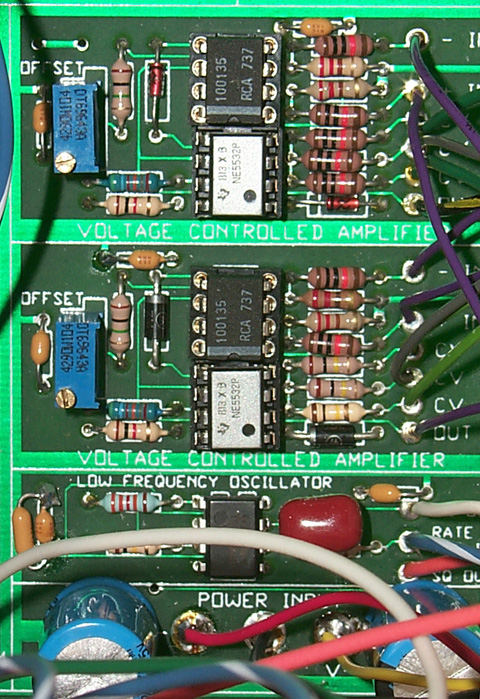
Closeup Picture (Contributed by Doug Ferrell 2000-02-02)
This module is pretty easy. Make sure to use normal diodes like the 1N4148 or 1N914. The op-amp can be anything dual - TL082, LM358, 1458, etc. There may be some hi-frequency oscillation on the VCA output - if there is, add about a 30pF cap across the (-) input and output on the output amp, across the 560k resistor. You can solder this on the back side if you want.
The control inputs again can be whatever you want, with 100k as the standard. It's a good idea to have the Initial Gain pot go a little negative when you turn it down all the way, so that the VCA shuts off completely. This way you can make the turn-on voltage from another module a little higher than zero volts.
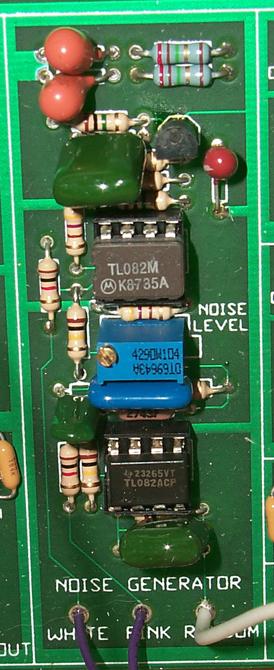
Closeup Picture (Contributed by Doug Ferrell 2000-02-02)
This circuit uses a reverse-biased NPN transistor as the noise source. This provides good clean wideband white noise in its purest analog form - the only problem is that it's a really tiny signal and needs lots of amplification. The subsequent op-amp stages boost the noise level and also provide the filtering for White, Pink and Random Noise outputs. The +/-15V supplies for these op-amps are filtered by a pair of RC networks (composed of the 22 ohm/10uF components) because even the tiniest hum in the power supply lines can make it through to the noise output due to the extremely high gains involved. You can play around with these values, but the values shown worked fine for my power supply.
Closeup Picture (Contributed by Doug Ferrell 2000-02-02)
This circuit ise used to buffer an external CV and add glide (portamento) to it. The first buffer is there to guarantee a low impedance source for the glide pot, and the second buffer follows the cap voltage and provides a low impedance drive source to control the VCOs, VCF and whatever else. As built it will provide exponential portamento (like on an Odyssey, 2600, Multimoog, etc.). It can be modified as shown in the drawings to provide linear portamento (like on a Minimoog, Pro Soloist, etc.). A trace cut on the solder side of the circuit board is required for this.
Closeup Picture (Contributed by Doug Ferrell 2000-02-02)
All capacitors that are not on the schematic are power supply bypass capacitors. Their value is shown on the assembly drawing as 0.1uF. (Notice that there are a couple 0.1 uF caps in the noise source - these are not bypass caps so I'm not talking about those here.) You can use 0.1 uF or 0.15 uF or whatever value fits that's not too much lower or higher. This is the one place that those el-cheapos ceramic caps are okay to use. Also, where the power wires are to be attached to the circuit board (at the lower rigth corner as you look at the component side with the writing on the silkscreen rigth-side-up), there's places for bigger caps. I used 1000 uF 16 V electrolytics here. Use whatever you want, just don't go below 16 V and fer heaven's sake don't put them in backwards because they WILL blow up with much smoke and flames.
If you know what you're doing, go for it. If not, stick with the recommended parts.
Temprature compensating resistors can be used in the positions shown. If you know about these, you can put them in. If you don't, just use normal metal film resistors.
All of the critical exponential converter components are physically placed next to each other so that they can be in physical contact. The transistors and the tempco resistors (if used) should be gooped up with heatsink compound (an insidious white paste) and tie-wrapped together, for best thermal result. This is totally optional and only for those who are after perfect performance. The result will be almost negigible so no big deal if you don't do it.
The capacitors over 1uF are polarized. The markings are on the assembly drawing. The diode polarities are on the circuit board silkscreen. The transistors on the VCF and Noise Source are standard E-B-C layouts on the silkscreen. The NPN transistors on the VCOs are marked for a MAT-02, but the holes are in E-B-C order. Examine the circuit traces to determine the proper orientation. The IC orientations are marked on the silkscreen. Note that the IC's in the VCA are "upside-down". All op-amp locations are marked "TL082", but you can ignore those based on the information above. Of course using all TL082s will work fine.
Included should be a big 11" X 17" drawing (Editors Note: this is really taken rigth out of the original paper works...) which is a blow-up of the silkscreen. On this I have marked all of the recommended component values. Once you have figured out what components you want to stuff, mark up the drawings to show this. Proceed to solder the components into the board. Here's the order in which I have done it:
You do NOT have to heat-sink anything. If you are not good at this, read the assembly section of a book like Craig Anderton's "Electronics Projects for Musicians". This is excellent info that applies here.
Most of the parts aren't very static-sensitive, with the exception of the CMOS parts and especially the CA3140s (that's why they get soldered in last). Be careful with those.
You can use sockets for the IC's if you want. I prefer to solder everything in, mainly because chips in sockets do tend to work loose over time and many cause flakey behaviour.
Some drawings have been included (Editors Note: This is taken from the original paperwork from Gene and is not yeat available in this webversion) to indicate the minimum recommended panel connections. I would consider the absolute minimum number of panel pots to be:
| VCO 1 | Fine Tune |
| Coarse Tune | |
| Initial Pulse Width | |
| VCO 2 | Fine Tune |
| Coarse Tune | |
| Initial Pulse Width | |
| VCF | Cutoff Frequency |
| Resonance | |
| ADSR 1 | Attack |
| Decay | |
| Sustain | |
| Release | |
| ADSR 2 | Attack |
| Decay | |
| Sustain | |
| Release | |
| VCA 1 | Initial Gain |
| VCA 2 | Initial Gain |
| LFO | Rate |
| Glide | Portamento Amount |
The Coarse Tune pots on the VCO could be octave rotary switches if desired. You may even be able to get rid of the Fine Tune pots if you use 10-turn or 20-turn panel pots for the Coarse Tune.
As for any additional controls - there's two primary approaches to modulation routing in modular synthesizers - I'll call them the "Moog approach" and the "Emu approach". The Moog approach is to put all the minimum pots on each module, and dealing with modulation depths and signal strengths (really the same thing in a true modular) by the use of attenuators and mixers on separate panels. The Emu approach is to provide all of the minimum pots on each module, and then provide provide additional pots on each module as input level controls for the audio as well as the CV inputs. The modules become more complex and costly, but more self-contained. Whatever you want to do, feel free. The Emu approach will probably cost more and take up more panel space, and lots of pots will go un-used most of the time, but it sure is easy to make patches.
Several proposals have been done for ASM-1 frontpanels and here is some of them:
From Josh Brandt <mute@sidehack.gweep.net> I got this design of Christopher List <Christopher_List@Sonymusic.Com>:
![[Drool picture of ASM-1 frontplate]](asm1-3.gif)
Please find Christopher's site about that frontpage here.
From Tim Walters
![[Another drool picture of ASM-1 frontplate]](ASM1.gif)
As for what kind of pots to use, if you were to go with all linear taper pots the machine would be quite useable. You migth find that with linear pots the ADSR time constants controls are a little touchy on the millisecond end of things, for example. It's really up to the builder to determine this. The way I buy large quantities of pots is to search out the local surplus houses for something suitable, and take whatever I can get.
One trick that I have found especially usefull is to remove the V/OCT trimmers in the VCOs from the circuit boards, mount them behind little holes in the front panel, and run wires to the circuit board trimpot locations. You can get away with any physical package of trimpot if you do this, so you won't be restricted to the 3-hole in-line 0.10" spaced pattern of trimpot that's on the circuit board. The trimpots can be mounted behind the panel with epoxy, but be carefull not to glue the trimmer screw!
With regards to jacks and switches, again this is up to the builder to choose. Here's a list of what I think the advantages and disadvantages of various signal interconnection methods are:
Advantages
Disadvantages
Advantages
Disadvantages
Advantages
Disadvantages
Power the module with plus and minus 15 volts. It is assumed that builder knows how to provide this, and that it is well-regulated. Apply power to the power input pads at the lower rigth-hand corner of the circuit board.
It is possible to build, test and use this circuit board without an oscilloscope, but I'd never do it. Be forewarned.
Once the board is powered up, you can sweep the VCO frequency using the INIT FREQ trimpot. You should see a sawtooth waveform at the SAW OUT pad, and a fairly square rectangular wave at the SQ OUT pad. You can leave this trimpot wherever you want.
If your VCO does not oscillate, ensure that the V/oct sum op-amp output is near 0V (to start of with, it should give about 900 Hz). If this does not help and the sawtooth output stationary at +15V you should try out making the 20 pF cap near the LM 311 somewhat larger, this will make the reset time for the capacitor longer and hopefully enougth to get back down to 0V. If this does not help, please check if your FET is correctly attached and ofcourse check the correctness of the rest of the curcuitry.
The scale calibration is adjusted with the V/OCT trimpot. This can be done as with any other analog VCO. Precise instructions for this are beyond the scope of this document.
Note that external frequency and Q pots are required for testing. The scale calibration is adjusted with the V/OCT trimpot. This can be done as with any other analog VCF. Precise instructions for this are beyond the scope of this document. One thing to note however is that this calibration is easier if the Q is set to maximum.
The two OFFSET trimpots are used to minimize the control voltage feedthrougth of each of the two integrator stages. With Q set to minimum, these pots are adjusted so that when the coarse frequency control is adjusted througth its full range, the deflection at the lowpass output is minimal. Set both pots at their midpoint to start with, then alternately adjust them until the deflection is at a minimum.
The OFFSET trimpot is to be adjusted for zero volts at the VCA optput with one of the control inputs at +5 volts and the other two unconnected.
The GATE THRESH trimpot is adjusted to provide the reference point above which the incoming gate signal must exceed to trigger the ADSR. You can set this to 1 volt for example, so that any input above 1 volt will trigger the ADSR. The range of adjustment goes up to 15 volts.
The ATK PEAK trimpot is adjusted to set the level at which the attack of the ADSR stops and the decay portion starts. If this is set too high, the ADSR will attack up to max and stay there. If this is set too low, then the ADSR peak will be lower than the sustain portion and the ADSR will decay up to it!
The SUS TRIM trimpot is adjusted so that the end of the attack phase and the maximum sustain level are at the same voltage. This will allow tweaking to true ADSR shape. You can set it otherwise and tell people that your ADSRs have a unique sound is you want, but of course you can do that with all the trimpots anyway.
The NOISE LEVEL trimpot sets the gain of the second stage of amplification in the noise generator. It can be set from nothing to clipping, so listen to the noise while adjusting it and put it where you want.
For everyone who has trouble sleeping in the nigth and needs some more booring facts I now bring you some insight on how the schematics below where brougth into their distribution format. I sit at home with my Linux machine hacking Postscript commands in Emacs, merges the page specific code with my Postscript library for electronic schematics using such heavy utilities as make and cat. I display the output using Ghostview and lately gv. Some people consider this (and they are probably rigth) a bizzare way of doing things, but in lack of a good and free tool that runs on my box I think that this is a good semi-optimum solution. The new PDF files where converted from Postscript using ps2pdf.
Whenever I have finished of my current hack-project (merging code for the mrouted 3.9 release) from the top of my desk I will see if I can't have a few more schematics going in here. After all is these two the most tricky one's.
The original VCO and VCF PDF files was kindly converted from my PS files by Tim Godfrey <tgodfrey at unicom dot net>. However, I recently converted them myself (since I now can do this) and put up the new files for people to use instead.
To view PS (Postscript) files I can recommend Ghostscript and Ghostview. For PDF files there is several free viewers and there Ghostscript and Ghostview also can help. For printing can however the PS files be good.
This section is devoted to the masters own usage to the ASM-1. Hopefully you will get inspired by this content. Gene's corner opened up on the late evening of 2nd Nov. 2002 after a cool gig hand hangaround with the band "Halv kokt i folie", to which I eventually intend to introduce the ASM-1 in real life.
![[Huge banana jack ASM-1 modular]](bananamodular6.jpg)
This one is a banana-jack modular that I made a couple of years ago. It contains five ASM-1's! All panels are laser-printed paper, laminated, trimmed, and drilled. Here is a description:
![[ASM-1 with Christopher List frontplate]](asm1-5.jpg)
This is my ASM-1 built behind one of the famous Chris List front panels. Under it is a JKJ CV-1 MIDI-CV converter.
![[ASM-1 prototype top view]](prototypetop.jpg)
This is one of the two prototype ASM-1's that I made to test out the artwork and the PCB fabrication house. I had a 748/308 op-amp instead of a TL082 for the pulse width comparator. This is the component side view.
![[ASM-1 prototype bottom view]](prototypebottom.jpg)
This is the solder side of the prototype. Notice that there were several artwork errors corrected with red wires. This is to be expected when you lay out PCB artwork without doing the schematic capture to go along with it and doing the netchecks. Pretty good for a first attempt? No, kind of careless actually, but I didn't care...
![[ASM-1 prototype top view]](productionversiontop.jpg)
Production ASM-1 stuffed, top view.
![[ASM-1 prototype bottom view]](productionversionbottom.jpg)
Production version stuffed, bottom view.
![[Tempcos and LM394]](parts3.jpg)
Three different tempcos and an LM394 (MAT-02 substitute)
An Evreka Advanced search on "ASM1 or ASM-1" gave 503 hits, not all apply ;) You will hit into a Gene search engine among other things, this must be the ultimate proof that building an ASM-1 is in the genes of some (it not all) of us. One definite side track is the Japanese missile ASM-1, which ceretainly knows how to make a cracking sound ending in a big bang. Many hits is however more or less electronics related, so you might bump into goodies that you not intended to... we even made it into Yahoo! Home : Entertainment : Music : Instruments : Keyboard Instruments : Synthesizers and Samples: Makes and Models
An little encyclopeadia that just got out may help someone. Incredibly broken and lacking a lot.
The ASM-1 has started to appear on recorded material, just to prove it's usefullness in real life.